Upon completing the first year of my degree, I was enthusiastic to continue studying materials science, alongside physics, in greater depth. Luckily for me, I thoroughly enjoyed both of the subjects that I was studying, however this made the decision regarding my third year subject choice all the more difficult. The opportunity to
spend my summer working in a materials research group was not one to be missed, since it helped me make the right choice for the third year of my degree (materials – obviously!), and allowed me to take a leap in personal development.
Having spent my last summer working in a research facility in Germany, I wanted to explore a new European country that I had not visited, but had always been drawn to – Switzerland. My arrival to Zürich was greeted with sunshine, and I instantly fell in love with the city. Alas, beautiful weather does not help with understanding Swiss German, which, as it turns out, is very different from the German I had learned in school. Fortunately, a lot of people spoke English, since Zürich attracts people from all over the world.
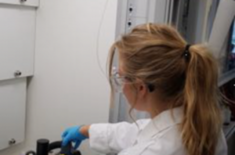
The research group that I was working with (Laboratory of Metal, Physics and Technology - LMPT) had researchers from all over Europe, who created a supportive work environment. To my surprise, I found that another student from Cambridge had come to the same research group and we were given a joint project to work on. Our project was titled ‘Mechanical strengthening of new aluminium-based alloys via structural manipulation’, the motivation of which was to find a cheaper alternative to aluminium-scandium alloys. After a week of reading papers and familiarising ourselves with the topic, we started the experimental part of our placement. The first half of the project was very routine, since it involved 20 heat treatment steps (each 3 hours long) after each of which the sample needed to be ground and polished to measure hardness. Though a lengthy process, it gave us more time to work on the literature review and have one or two coffee breaks (which are an essential element to any ground breaking research).
The second half of the project was focused on sample preparation for or TEM (Transmission Electron Microscopy) and APT (Atomic Probe Tomography) via rapid solidification processing, namely wire spinning and melt spinning. After spending a few weeks optimising the parameters of the wire spinner, melt spinner and electropolishing machine, we embarked on a journey to find electron transparent regions in our sample under the TEM. Even though some samples had failed and it took hours to find transparent regions in others, we managed to acquire a selection of beautiful TEM images.
When I was not in the lab, I made sure to explore as much of Switzerland as possible. Three other students from Cambridge were working at ETH that summer, and we travelled somewhere new every weekend. This placement has been an incredible opportunity for personal growth, as well as fun adventures, for which I am infinitely grateful. I would like to thank the Gateway Programme, Murray Edwards College, University of Cambridge and ETH Zürich for making this experience possible. I’d also like to thank Prof. Dr. Löffler, Dr. Schäublin, Dr. Stoica and Viktor Wessely who have supported me throughout the whole project, as well as Štefan Stanko for being a great lab partner.
Ekaterina Kaliteevskaya
Natural Sciences (Physical)